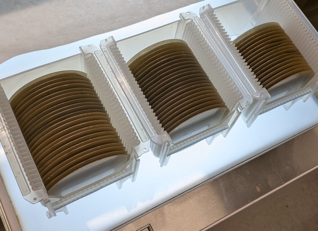
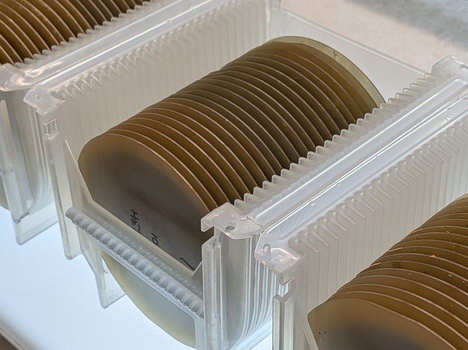
Crystal IS has produced its one hundredth 100 mm bulk Aluminum Nitride (AlN) wafer from its new 100 mm pilot-production line. With an initial capacity of 1,250 substrates a year, this pilot line achievement demonstrates the yield, uniformity, and repeatability at scale of Crystal IS’ bulk AlN platform for next-generation high-performance electronic and optoelectronic devices.
Since 2023, Crystal IS has been collaborating with leaders in ultrawide bandgap semiconductor development—supported in part by government initiatives such as the NITRIDER program within the NORDTECH hub of the Microelectronics Commons. These initiatives reinforce the national push to strengthen domestic semiconductor manufacturing and accelerate innovation across aerospace, defense, research, and commercial sectors. The growing adoption of AlN highlights the value of sustained public-private collaboration in securing U.S. leadership in advanced electronics.
“Crystal IS was founded on the promise of bulk AlN technology. Our ability to achieve this 100 mm wafer benchmark confirms the robustness of our processes and expertise at 100 mm, and ability to scale to larger diameters” said Eoin Connolly, President & CEO of Crystal IS “This milestone is an important step toward enabling high-power, high-frequency devices for optoelectronic, RF and power applications that benefit from the intrinsic performance advantages of native AlN.”
In parallel with scaling wafer production, multiple partners have now demonstrated advanced GaN- and AlN-based HEMT devices on Crystal IS bulk AlN substrates using both MBE and MOCVD growth techniques.
Cornell University recently published results of their new XHEMT architecture grown on bulk AlN from Crystal IS which showed substantially fewer defects than traditional GaN-on-Si, GaN-on-SiC, or GaN-on-Sapphire. “These defects can propagate all the way through a device, whereas our new aluminum nitride substrate basically eliminates them,” said Dr. Grace Xing, William L. Quackenbush Professor of Engineering at Cornell University. “While this needs to be studied in more detail, I think it will translate to a tremendous advantage in the upcoming iterations of this device.”
“By integrating large diameter AlN substrates with novel AlN/GaN/AlN XHEMTs, we aim to bridge the gap between fundamental materials research and scalable device fabrication for next-generation RF power amplifiers for radar and communication systems,” said Dr. Debdeep Jena, Professor of Electrical and Computer Engineering and Materials Science, Cornell University. “The availability of 100 mm AlN at volume is a critical milestone to this effort.”
AlN: A Platform for the Next Generation of Power and RF Electronics
Crystal IS’s low-defect density bulk AlN substrates offer significant advantages for high-power, high-frequency and high-temperature electronics:
- High thermal conductivity
- Excellent lattice match for GaN and Al-rich III-N epitaxy
- Reduced defect formation in high-Al-content HEMT structures
- Improved reliability and long-term device stability
The new pilot line support U.S. supply chain readiness for next-generation high-performance, radiation-hardened, high-temperature electronics. With this achievement, Crystal IS supports US dominance in AlN substrate manufacturing for optoelectronics and emerging RF and power device requirements.
“As industry demand grows for higher power densities and greater efficiency, native AlN is emerging as the material of choice,” said Kasey Hogan, Product Manager for Substrates – RF and Power Devices at Crystal IS. “Our progress at 100 mm puts us on a clear path toward the next level of scalability and device performance.”
The new pilot production line in Green Island, NY has an initial capacity of 1250 100 mm substrates per year, scalable to 10,000 per year. The company will continue to support its existing 2” production line for optoelectronics while expanding its capabilities to meet growing demand for larger-format wafers.
Acknowledgment: This prototype was partially supported by the Microelectronics Commons Program, a DoW initiative, under award number N00164-23-9-G061.